Furtak Research Projects
Plasmonic Device Physics
The electrons at the surface of good metals can oscillate in a collective wave that is also coupled to an electromagnetic excitation. These so-called surface plasmons have some unique charateristics. The are a hybrid excitation that can be guided by the contour of the metal, and the fields at the surface of the metal can be very large. We are studying the theoretical and experimental aspects of plasmonic structures for enhanced chemical detection, improved electromagnetic detectors, and specialized optoelectronics.
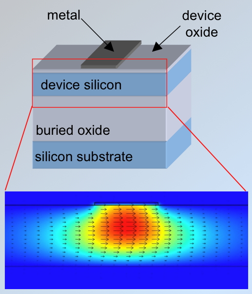 Data processing of plamonic signals traveling along metal waveguides would lead to high bandwidth electronics, since the frequency of surface plasmons are very large, compared to what is possible with electronics based on movement of charge carriers. However, a serious limitation of plasmonic waveguides is that the excitations don't propagate very far because of ohmic losses in the metal. We have discovered a possible solution to this problem using a design based on a standard silicon-on-insulator (SOI) wafer. A metal strip on top of the thin device oxide modifies the optical properties of the crystalline device silicon under the oxide so as to enable waveguiding. The contour plot shows the spatial distribution of the mode. Most of the field energy is in the silicon where losses are minimal.
The properties of the mode are very sensitive to the thickness of the device oxide and the width of the metal strip. The mode can be adjusted to localize the fields very near to the metal, or to optimize the propagation length. Our modeling shows that macroscopic distances beyond 30 cm should be achievable. This is considerably farther than what can be achieved with other plasmonic waveguide configurations. These structures are simple to fabricate and can be built into a variety of cavities and resonant structures.
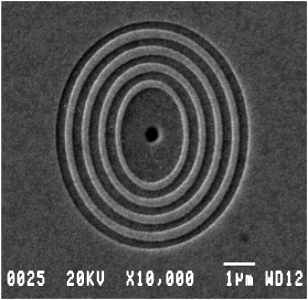 Plasmonic cavities can be used to channel incoming electromagnetic radiation to an optoelectronic detector. The structures are sufficiently small that the device can form a single pixel in a detector array. This electron micrograph shows an oval-shaped cavity that is preferentially sensitive to polarized light. We are using this concept to design imaging polarimeter detector arrays. The polarization characteristics of light can be used to distinguish the material properties of the source, such as the difference between a metal and a non-metal.
This research, which is funded by the Air Force Office of Scientific Research, is a collaboration between CSM and ITN Energy Systems. The partnership at Mines is lead by David Flammer and includes Reuben Collins, and Chip Durfee. You can learn more about our projects by visiting our Plasmonics web site.