EENG 383
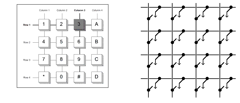
KeypadsGiven its function, you might expect that all the switches in the 4x4 keypad would have one side tied together in a common line and present the other line as an external signal. These 16-lines would consume a significant number of MCU pins. Luckily there is another organization which requires only 1/2 the number of external signals.
There are 8 external signals used to access a 4x4 keypad. These 8 signals are arranged in 4 rows and 4 columns. Pressing a button in row i and column j causes the ith row signal to be connected to the jth column signals. This hardware arrangement is shown in the figure below.

Before we answer the question of how to read which key is pressed, we need to interface the keypad to the MCU. This is done as follows:
- 1 pull-up resistor is added to each of the 4 columns. Thus, when no keys are pressed all the columns would read logic 1.
- Each of the 4 columns is run to a MCU input - the MCU will read these pins to determine which key was pressed.
- The rows are connected to MCU pins. At any one time only one of the MCU pins will be an output (asserting logic 0), while the other three pins will be configured as inputs.
| Key press | r1,r2,r3,r4 | c1,c2,c3,c4 |
| none | in,out,in,in | 1,1,1,1 |
| 1 | out,in,in,in | 0,1,1,1 |
| 4 | in,out,in,in | 0,1,1,1 |
| 1,4 | out,in,in,in | 0,1,1,1 |
| 1,4 | in,out,in,in | 0,1,1,1 |
| 5 | in,out,in,in | 1,0,1,1 |
| 9 | in,in,out,in | 1,1,0,1 |
| 5,9 | in,out,in,in | 1,0,1,1 |
| 5,9 | in,in,out,in | 1,1,0,1 |
- Not be able to distinguish which key was pressed. If all the rows were outputs asserting logic 0 then column 1 would output a 0 whenever any of the keys in the first column were pressed. We couldn't know which because all the row outputs are the same. Hence, some of the row outputs would have to be different.
- Create short circuits. If we pressed both buttons in the rows which output different values then the opposing outputs would be connected to one another.
Firmware
I'd build this firmware on top of a timer interrupt which triggers every 50mS (200mS to read entire keypad).
// global where each bit
int16	keypad;

void INIT_PIC() {
    keypad_row = 0;		// assert "0" on all rows
} //

void ISR() {

    static int8 row_tris = 1;	// the tris bits for the keypad row
    static int16 mask = 0x000F;	// used to mask bits of global var keypad
    static int8 shift = 0;	// Used to shift the column bits into position

    tris = ~row_tris;		// assert a "0" only on one row
    keypad &= ~mask;		// clear out the old key values
    keypad |= col << shift; 	// mask in the new ley values

    shift += 4;			// next shift needs to accomodiate 4-bits
    if (shift > 12) shift = 0;	// and roll-over

    row_tris = (row_tris << 1) & 0x0F;
    if (row_tris == 0) row_tris=1;

    mask = mask << 4;
    if (mask == 0) mask = 0x0F;

} // end ISR