EENG 393
In Lab 4 - PSU operationRequirements
When you have worked through all the material in this lab writeup, please take the inLab 04 Quiz. You may find quiz questions to be similar to, but not identical to the numbered questions in this inLab write up. Note, you wil have 60 minutes to complete the ten questions in the Canvas quiz so it would be a good idea to complete all the inLab activities before taking the Canvas quiz. Do not turn in the answers to the numbered questions in this inLab writeup.Power Supply Analysis
Regulation is the act of maintaining a constant voltage or current at a circuit terminal regardless of how the input or load changes. We are building a linear power supply which are characterized by:- Having output voltages that are less than input voltage,
- Not power efficient,
- Dissipate lots of heat,
- Provide very stable voltage and current output,
- Respond quickly to changes in the load.
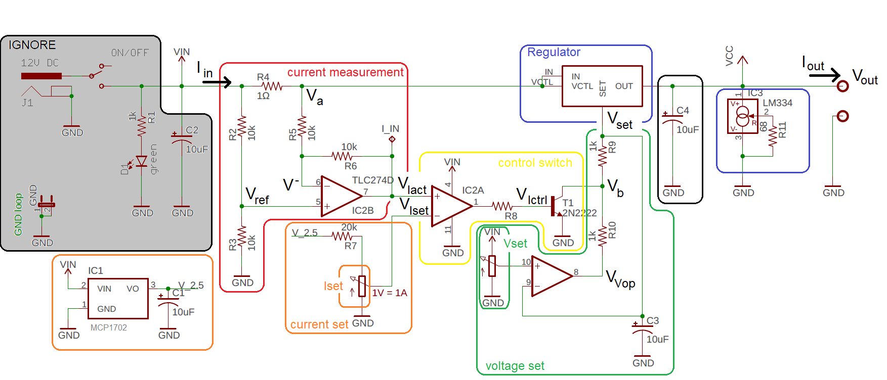
The operation of this power supply is identical to the bench top power supplies. The user sets a maximum voltage and current using the two pots labeled "Iset" and "Vset" in the image above. What follows are several important observations that you will need to keep in mind as you walk through an analysis of this circuit.
- Iout = Iin (well almost). While this may seem counterintuitive at first, there are no significant paths to ground for current from the input to output,
- The current measurement block's job is to create a voltage (in volts) that is equal to the current (in amps) flowing through R4, the 1Ω current sense resistor. In other words, VIact is proportional to Iout,
- The LT3080 tries to set its OUT pin to the same voltage as its SET pin,
- If Iout < Iset then the transistor T1 does not affect the voltage set feedback loop. This then allows the user selected Vset to be applied to the SET pin of the LT3080,
- If Iout > Iset then the transistor T1 grounds the Vset signal causing the LT3080 to output 0V. This will quickly cause the Iout < Iset turning the LT3080 back on. This will quickly cause Iout > Iset. The capacitor C3 smooths out these transitions resulting in Iout == Iset.
Operational Amplifier
Operational amplifiers (op-amps) play a major role in the design of our power supply and you will find them to be one of the most commonly used active components in electronics design. The fact that there are 1000's of different op-amps, means that they have been optimized for a myriad of different electronics tasks. We will be using the Texas Instruments TLC274 quad op-amp. The term "quad" means that the IC contains 4 independent op-amps. Each of the four op-amps is drawn using the following figure.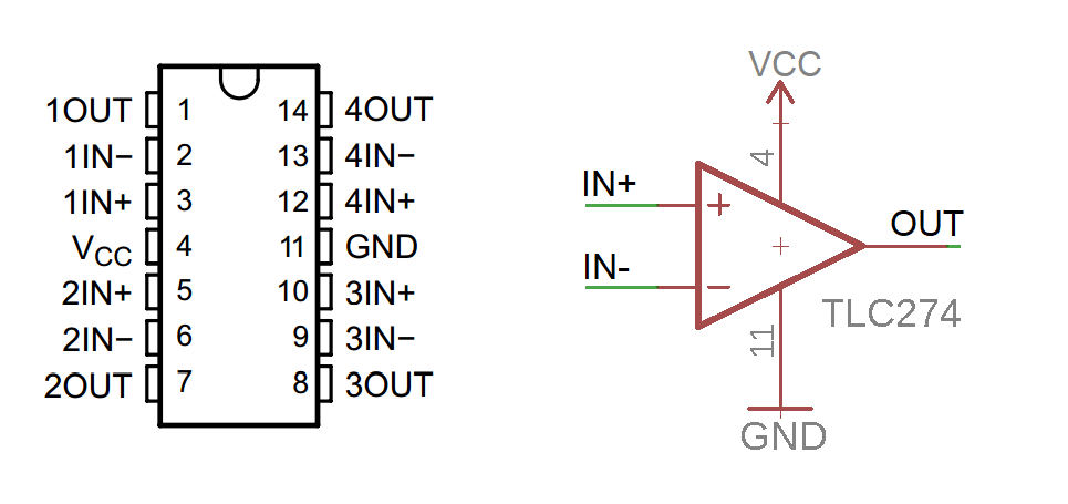
The Vcc and GND inputs provide power to the op-amp. The supply voltage can be anywhere from 4V to 18V. Each op-amp on the chip has two inputs, IN- the inverting input and IN+ the non-inverting input, and one output OUT. An important quality of op-amps is that very little current flows into their inputs. In most cases you can assume that no current flows into the inputs. Each of the four op-amp on the chip is numbered [1 … 4]. The relationship between the inputs and output of an op-amp is summarized as follows:
    OUT = AVD*(IN+ - IN-)
    as a consequence of this fact is follows that:

    if (IN+ > IN-) then OUT increases towards VCC
    if (IN+ < IN-) then OUT decreases towards GND
Before we examine two common op-amp configuration a few points need to
be made:
- No current flows into the IN+ and IN- inputs,
- The open-loop gain AVD is somewhere around 40,000
	If (IN+ > IN-) then OUT = VCC
	If (IN+ < IN-) then OUT = GND
This op-amp configuration is called a comparator, because the op-amp is comparing its inputs and the output reflects which is larger.
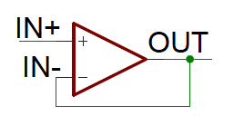
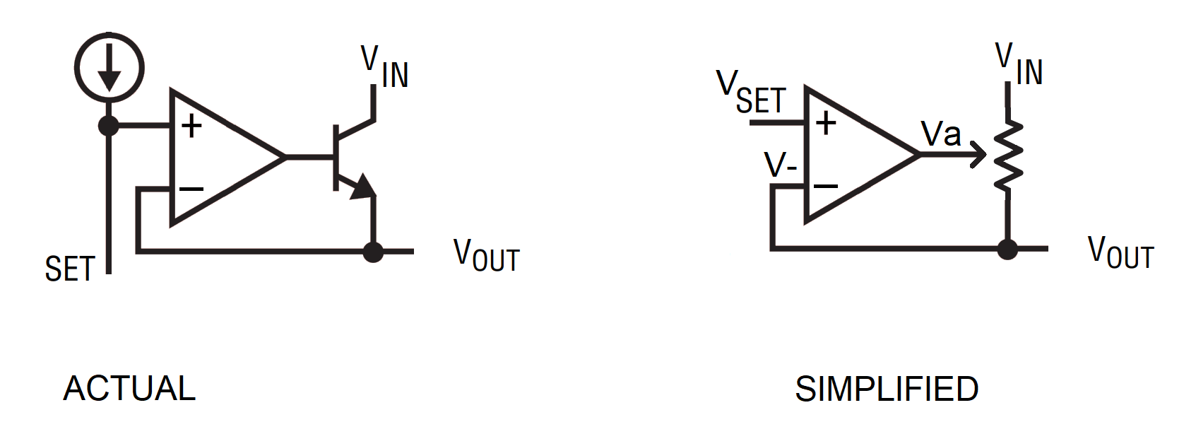
Negative Feedback One particularly useful op-amp configuration is shown in the image below, connecting the output to the inverting input. A connection from the output to the inverting input of an op-amp is called negative feedback.
-
Complete an analysis of this configuration by filling in
"increasing" or "decreasing" in the blanks below. Carry over
the answer from one line to the following line.
If IN+ > IN- then OUT
If OUT        then IN-       .
If IN-        then the difference between IN+ and IN-       .
-
If IN+ < IN- then OUT
If OUT        then IN-       .
If IN-        then the difference between IN+ and IN-       .
- Given that the difference between IN+ and IN- does the same thing in both of the above cases, what does IN- equal?
BJT
We could teach a whole course on bipolar junction field effect transistors (BJT) and still not cover all their interesting applications. No doubt that you have come across a few in your studies as an EE. For today, I am going to use a simple model of a BJT that works for a large portion of circuits that you will analyze. The following figure shows that this SIMPLIFIED model, places a variable resistor between the collector and emitter.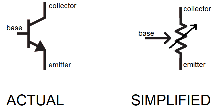
Call the voltage on the base Vb and the resistance between the collector and emitter RCE. The relationship between these two quantities is given by the following:
As Vb increases, RCE decreases towards a short circuit
As Vb decreases, RCE increases towards an open circuit
Note in the limit, when Vb is at the supply voltage, RCE decreases to very low resistance, neat 0Ω On the other hand as vb is at ground, the RCE increases to very high resistance, neat ∞Ω In this scenario, the BJT is acting like a switch and will be replaced by one is a simplified version of the circuit.
LT3080
The LT3080 is a linear voltage regulator that we will trick into perform current regulation also. It is shown in the blue block in the architecture above (along with the LM334 - more on that later). The LT3080's operation is very easy to understand, the output voltage is equal to the voltage on the set pin. To understand the behavior better, open these technical documents for the LT3080. Before proceeding to the following questions note that the minimum difference between the output voltage and the input voltage is called the drop-out voltage. This represents the minimum amount of "headroom" that you need in order for the linear regulator to operate.- What is the maximum output current of the LT3080?
- What is the drop-out voltage?
- What is the minimum load current?
The current sources shown in the LT3080 technical documents is a 10µA source that is normally used (when combined with an external resistor) to set the control voltage, SET. We are going to force a voltage on this pin using an external circuit that will have no problem sinking this 10µA of current. So I tossed out the current source in the simplified model. Next I replaced the BJT with an "equivalent" variable resistor. Finally I renamed some of the nodes in the circuit with names that you will use in the subsequent analysis.
-
Complete the following analysis by filling in the blanks with
"increases" or "decreases" as appropriate. Carry over the
answer from one line to the following line.
If Vset > V- then Va
If Va        then RCE       .
If RCE        then V-       .
If V-        then  (Vset - V-)       .
- Complete the following analysis by filling in the blanks with
"increases" or "decreases" as appropriate. Carry over the
answer from one line to the following line.
If Vset < V- then Va
If Va        then RCE       .
If RCE        then V-       .
If V-        then  (Vset - V-)       .
- From this analysis, what is the relationship between Vout and VSET?
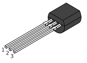
- Which pins of the LM344 (V+, R, V-) go to which pins of the
following TO-92 package (1, 2, 3)?
- Look up Figure 11 to determine the set resistor value that generates 1.0mA of current.
Current measurement
While there are several different ways to measure current flowing through a load, Iload in the following image, we will use a current sense resistor. The idea is very straight forward and illustrated in the following diagram.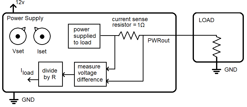
The user (you) will use a pair of potentiometers to limit the maximum current and voltage supplied to the load, Vset and Iset in the image above. The LT3080 will be responsible for limiting the current and voltage; its denoted by the "power supplied to load" box in the image above. This power will run through the 1Ω current sense resistor. Using Ohm's law, the voltage drop across this resistor, Vdrop, is equal to the current through the resistor times 1.
Differential amplifier The circuit that measures the voltage difference across the current sense resistor is called a differential amplifier. So named because the circuit measure the difference between two signal levels. While you can purchase a purpose-built differential amplifier, we will build one using an operational amplifier (op-amp) because we already have an op-amp chip in our circuit and rather than add another chip to the circuit, we will use an op-amp that is already there.
The structure of our current sense resistor and differential amplifier is shown in the following image.
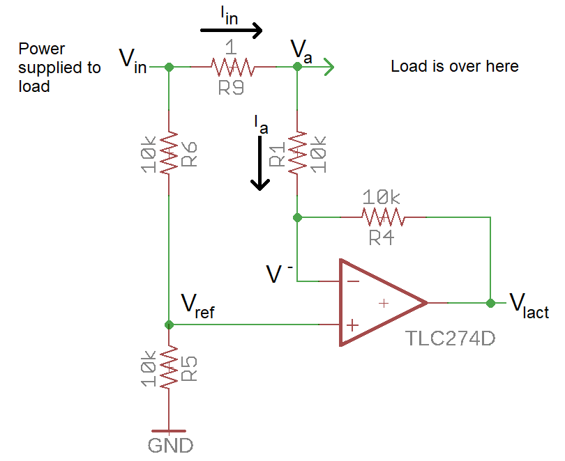
You will be able to analyze the op-amp circuit in the previous image using a few helpful facts.
- The "power supplied to load" has a voltage of Vin,
- The "power supplied to load" has a current of Iin,
- The op-amp will manipulate its output in an attempt to make the voltage on its inputs the same,
- No current flows into the op-amp inputs,
- The current sense resistor is 1Ω,
- Ohm's law.
- Write an Ohm's law equation for the voltage drop across the current sense resistor (Vin - Va) in terms of Iin and the value of the current sense resistor.
- Solve the previous equation for Va.
- Write an equation for the voltage on the non-inverting input of the op-amp (Vref) using the variables: Vref, Vin,
- Can the op-amp directly affect the value of Vref by changing its output?,
- Write an Ohm's law equation for the resistor R1 in terms of Ia, V-, Va as well as the value of the resistor. Solve this equation for Ia.
- Can the op-amp directly affect the value of V- by changing its output?,
- Remember that an op-amp with negative feedback will manipulate its output in an effort to keep the voltage on its inputs the same. Write an expression for the voltage on the inverting input of the op-amp, V- in terms of Vin.
- Rewrite the equation for Ia (derived in a previous step) by replacing the Va and V- terms. Simplify the expression by performing subtraction of the Vin terms.
- Remember that no current flows into the inputs of an op-amp. This implies that all the current Ia will flow through the resistor connecting the inverting input to the op-amp output. Write an Ohm's law equation that relates the voltage at the op-amp output (VIact) using the variables: VIact, V-, Ia and the value of the resistor R4.
- Modify the expression for VIact derive in the previous step by replacing its V- and Ia terms with expression derived in a previous step that were in terms of Vin. Simplify the resulting expression until it looks like an Ohm's law equation.
Current set
The current set functionality consists of two components, a MCP1702 (HD type) voltage regulator and a voltage divider.- Pull the technical documents for the MCP1702. What is the voltage output of the MCP1702 (Using the part symbol HD - see Section 7.1 of the Tech Docs) the part.
- What range of load capacitor should be connected to the output?
- Go back to the power supply design for this question. Note the POT is 20kΩ. What range of voltage can you generate on the output of the current set potentiometer?
Voltage set
The voltage set portion of the circuit is just a op-amp with negative feedback drawn in an unusual way. Take a look at the following reproduction of this portion of the circuit.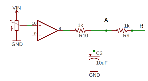
- Reference the Power Supply schematic at the beginning of this lab. What devices do points A and B in the image above, connect to?
Control switch
The control switch takes the output of the current measurement and current set and runs them into a op-amp setup in a comparator configuration as shown in the image below.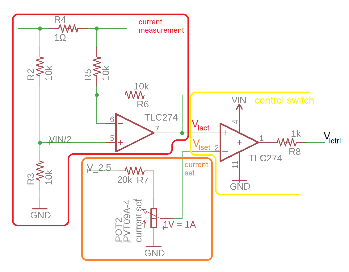
In our circuit the non-inverting input is the voltage which represents the current being delivered to the load Vcurr and the inverting input comes from a potentiometer adjusted by the user to dictate the maximum current to deliver to the load, VIset.
- Reinterpret the comparator behavior discussed to determine the output
of the comparator in the blanks below. Your answer should be "VIN" or
"GND"
	If (VIact > VIset) then VIctrl =
	If (VIact < VIset) then VIctrl =
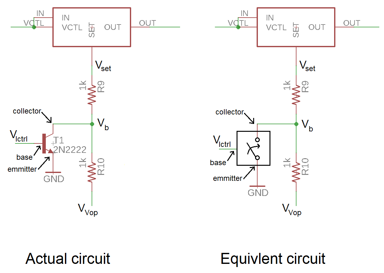
Use our earlier discussion of the equivalent circuit for an NPN transistor to answer the following questions. Your answers should be either "open circuit" or "short circuit".
- When the base of the BJT is held at the collector voltage (Vcc), RCE acts as a .
- When the base of the BJT is held at the emitter voltage (GND), RCE acts as a .
Let's reinterpret this NPN transistor's action in terms of the voltage at the set pin of the LT3080. To start, let's examine how the VIctrl voltage effects the voltage at the intermediate node Vb.
	If (VIctrl == VIN) then Vb = GND         // because the switch is closed
	If (VIctrl == GND) then Vb = VVop        // because the switch is open
The final step in the analysis is to assert that Vset is basically equal to Vb because there is only 10µA of current flowing out of the SET pin of the LT3080. Consequently, we can reinterpret the preceding characterization of how VIctrl voltage effects the voltage at the SET pin of the LT3080 Vset.
	If (VIact > VIset) then Vset = GND        // current limited
	If (VIact < VIset) then Vset = VVop       // voltage limited
This results deserves some explanation. Let's assume that user has configured the power supply in such a way that the power being supplied to the load is limited by the maximum current-level set by the user.
VIact > VIset:
In the first condition VIact > VIset, the load is receiving more current than set by the user. As a consequence the NPN transistor grounds the Vset pin of the LT3080. This causes the output of the LT3080 to decrease (towards 0V). As a consequence, the voltage delivered to the load drops causing the current delivered to the load to drop. This will eventually cause the current consumed by the load to drop below the current set by the user. This will transition the circuit to its other mode of operation.
VIact < VIset:
In the second condition VIact < VIset, the load is receiving less current than set by the user. As a consequence the NPN transistor is open-circuited, allowing the LT3080 output voltage to increase towards the level set by the user, VVop causing the current delivered to the load to increase. This will eventually cause the current consumed by the load to increase above the maximum current level set by the user. This will transition the circuit to its other mode of operation.
On the other-hand, let's assume that the user has configured the power supply in such a way that the power being supplied to the load is limited by the maximum voltage set by the user. In this case the NPN transistor will always be an open-circuit because VIact < VIset This will then cause Vset = VVop causing the LT3080 output voltage to be held at VVop volts.