EENG 393
In Lab 10 - Bill of Materials
Objective
Create manufacturing files for fabrication of your PCB. Have the
Lab Instructor or Teaching Assistant sign-off each of the items
below.
Common problems
- Included attribution on your PCB!!
- Your name
- Board name and revision
- Date
- Optional: Your company
- Name the test points with their signal names
(I_out, V_out, I_set, V_set) by renaming the test point in
your schematic,
- Label the VU meter switch positions settings,
- Check the inverting and non-inverting inputs on op-amp
IC3A in the schematic below and make sure that your
schematic is the same,
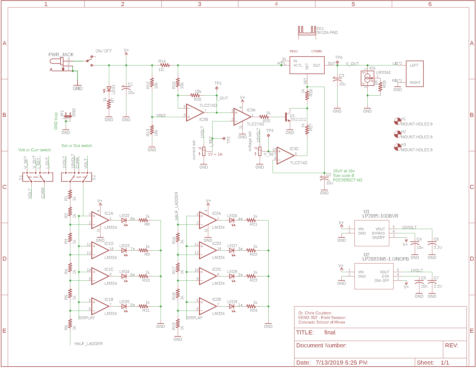
- The heat-sink must be adjacent to the LT30380 metal tab.
Pass Electrical Rule Check
There should be not major errors or warnings left in your schematic.
Pass Design Rule Check
Download
PCBway.dru into your project
directory. In layout window, make sure that you have run the
Ratsnet tool to flood fill with any copper pours
- Tools → DRC …
- In DRC pop-up, in the File tab, click Load…
- In the Load pop-up, navigate to the downloaded
PCBway.dru file, select it, click Open
- Back in the DRC pop-up, select Apply, then click Check
- When all the DRC errors are cleared, you will see
"DRC: No errors." in the lower left corner of the layout
window.
Generate Gerber Files
Gerber files are a hold-ver from the days when PCBs were
made by exposing photographic file to a light move by a
2-axis machine.
| Gerber file | Name | Included EAGLE layers
|
| layout.out | Outline file | 20
|
| layout.sst | Silk Screen Top | 21, 25, 27, 51
|
| layout.smt | Solder Mask Top | 29
|
| layout.top | Top copper | 1, 17, 18
|
| layout.bot | Bottom coppper | 16, 17, 18
|
| layout.smb | Solder mask bottom | 30
|
| layout.drd | Drill file | 44, 45
|
Before you continue, take a moment to determine the width and height
of your PCB in millimeters. You can switch the units in EAGLE layout
by selecting View → Grid. In the Grid pop-up select "mm" as the
size. Or you can just convert mils to mm, whatever you prefer.
- Download PCBway.cam into your
project directory,
- Create a folder named <your last name>
- File → CAM Processor …
- Click on the Load job file icon, select
Open CAM File …
- In the Select CAM file pop-up, navigate to the downloaded
PCBway.cam file, select it, click Open
- Back in the CAM Processor pop-up, click Process Job,
- In the Select output directory pop-up, click on the folder
named <your last name>, click Select Folder,
- Back in the CAM Processor pop-up, you should be
greeted with a CAM Exporter: process complete pop-up,
click Open folder,
- Open windows File Explorer,
- Navigate to your <your last name> folder,
- Right click on the folder and select Send to →
Compressed (zipped) folder …
Check Gerber Files
- Open thejlcpcb.com
web page,
- Click on the blue "Add your Gerber file" button,
- In the Open pop-up, navigate to your <your last name>
zipped folder,
- Double click on your <your last name> zipped file,
- The web page will show you your board,
- Click on the Gerber Viewer
link at the lower right of your PCB,
- On the Gerber View page, you can
- Move: Left mouse, drag
- Zoom: Center mouse, scroll up (or down), center mouse,
then move
The following are things that have been sent to out for
fabrication and been rejected by the manufacture. So,
check your gerber view for the following:
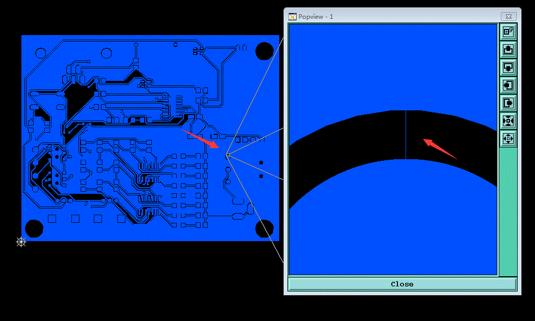
- Do you have drill files?
- Do you have tiny traces connecting GND/VCC pads
to your copper pour?
Upload your files
Please make a directory on your Google drive called "final revision"
containing your zip file created in the previous step. If I have
any problems uploading the designs, I'll get your design files
from your Google drive folder.
- Put your design files on a thumb drive and take them to the
podium computer that the lab instructor is logged into,
- Make sure that the browser is pointed at: https://jlcpcb.com/quote/#/
- Process instructions:
- Layers: 2
- Dimension: <Auto filled by next step>
- PCB Qty: 5
- PCB Thickness: 1.6
- PCB Color: <Choose your color>
- Surface Finish: HASL (with lead)
- Copper Weight: 1 oz
- Gold Fingers: No
- Material Details: FR4-Standard Tg 130-140C
- Panel By JLCPCB: No
- Flying Probe Test: Fully Test
- Castellated Holes: No
- Different Design: 1
- Specify Order Number: No
- SMT Assembly: No
- Stencil: No
- Click on the blue "Add your Gerber file" button,
- In the Open pop-up, select your zipped file, click Open,
- Wait for Processing Gerber files… to complete,
- In the PCB review page, click "Gerber Viewer",
- Verify design,
- Back on the order page, verify board color the click "Add to Cart"
- On the next page you should see a green check next to
"Success, this file has been saved to your File Manager",
- Click the link for File Manager,
- Verify that your file with PCB icon is shown.