EENG 383
Lab 10 - Audio recording and playbackRequirements
Working in teams of two, read through the following lab activity and perform all the actions prescribed. You do not need to document bullet items. Make a record of your response to numbered items and turn them in a single copy as your teams solution on Canvas using the instructions posted there. Include the names of both team members at the top of your solutions. Use complete English sentences when answering questions. If the answer to a question is a table or other piece of art (like an oscilloscope trace or a figure), then include a sentence explaining the piece of art. Only include your answers, do not include the question-text unless it is absolutely needed.Objective
To familiarize you with the digital to analog (DAC) conversion method that converts a PWM waveform into an analog waveform using a low pass filter.External Hardware
Take a moment to verify that the discrete component (capacitor and resistor) values from the low pass filter schematic (shown below) match those found on your development board.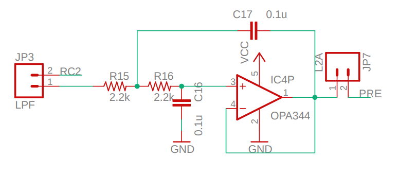
Look at Figure 2 at the wikipedia page on the Sallen–Key topology low pass filter. Note the wikipedia article refers to corner frequency as fo
- What is the calculated corner frequency of our (2nd order) low pass filter?
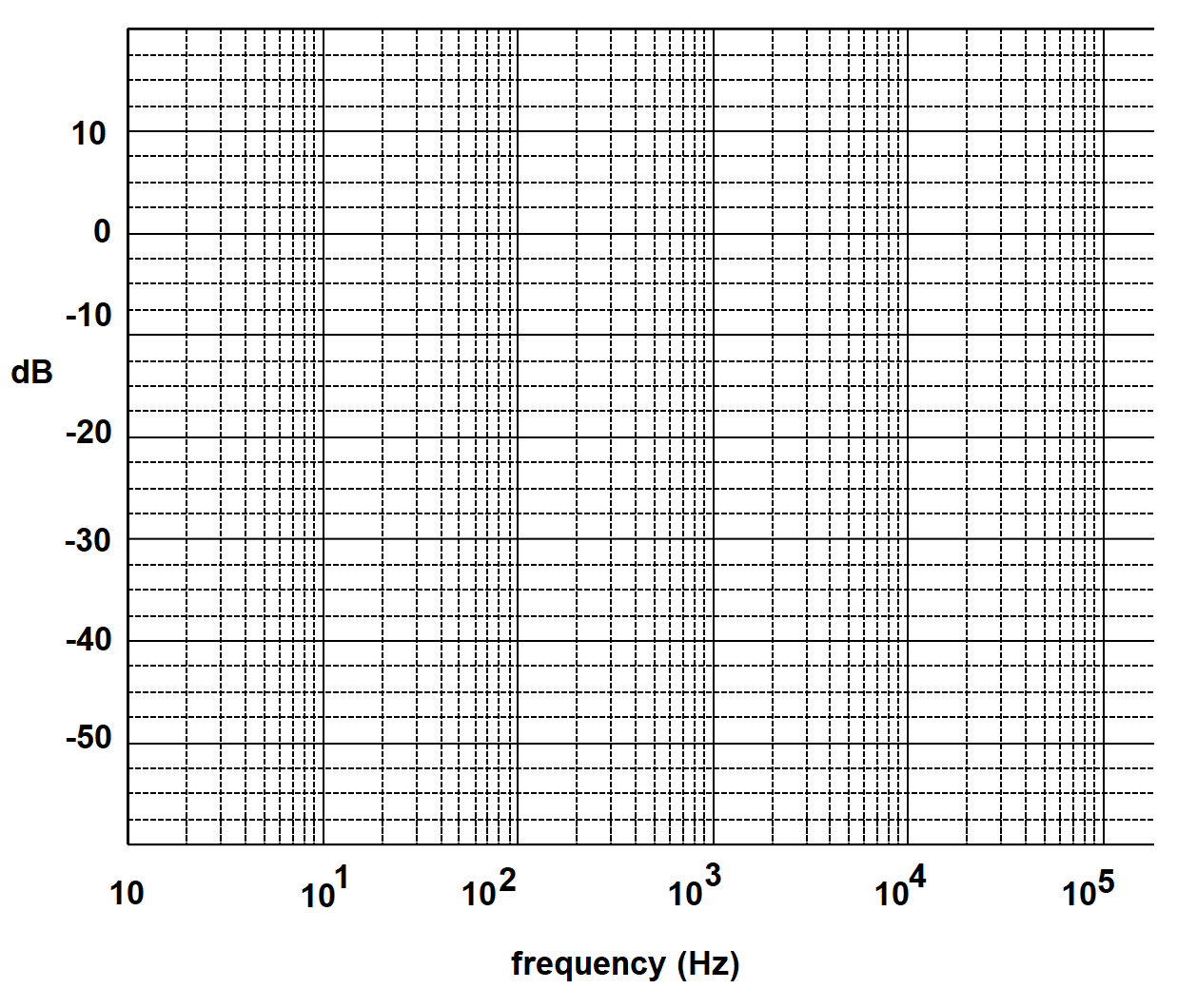
- Draw a rough (theoretical) sketch of the frequency response graph
for our second order low pass filter using the graph below.
- Connect a proper signal generator cable to the function generator yellow BNC connector labeled "CH1",
- If the [Sine] function key is not illuminated, press the [Sine] key to illuminate it,
- Press the [Amp] soft key twice to highlight "HiLevel",
- Enter 3.0 on the numeric keypad, and then press the "V" softkey
- Press the [loLevel] soft key once,
- Enter 0 on the numeric keypad, and then press the "V" softkey
- Press the [Freq] soft key once,
- Enter 1.0 on the numeric keypad, and then press the "kHz" softkey
- Connect a proper oscilloscope probe to the channel 1 input of the oscilloscope. Adjust the vertical scale to 1V/div and the horizontal scale to 500us, make sure that channel 1 is DC coupled, and that the trigger level is around 1.65V,
- Connect the function generator and oscilloscope cables, black clip to black clip and red clip to scope probe,
-
Adjust the scopes so that they display frequency and the peak-to-peak
amplitude of the waveform.
- [Meas] → Clear Meas → Clear All
- [Meas] → Source → 1 →
- [Meas] → Type → Peak-Peak → Add Measurement
- [Meas] → Type → Freq
- [↑ Back]
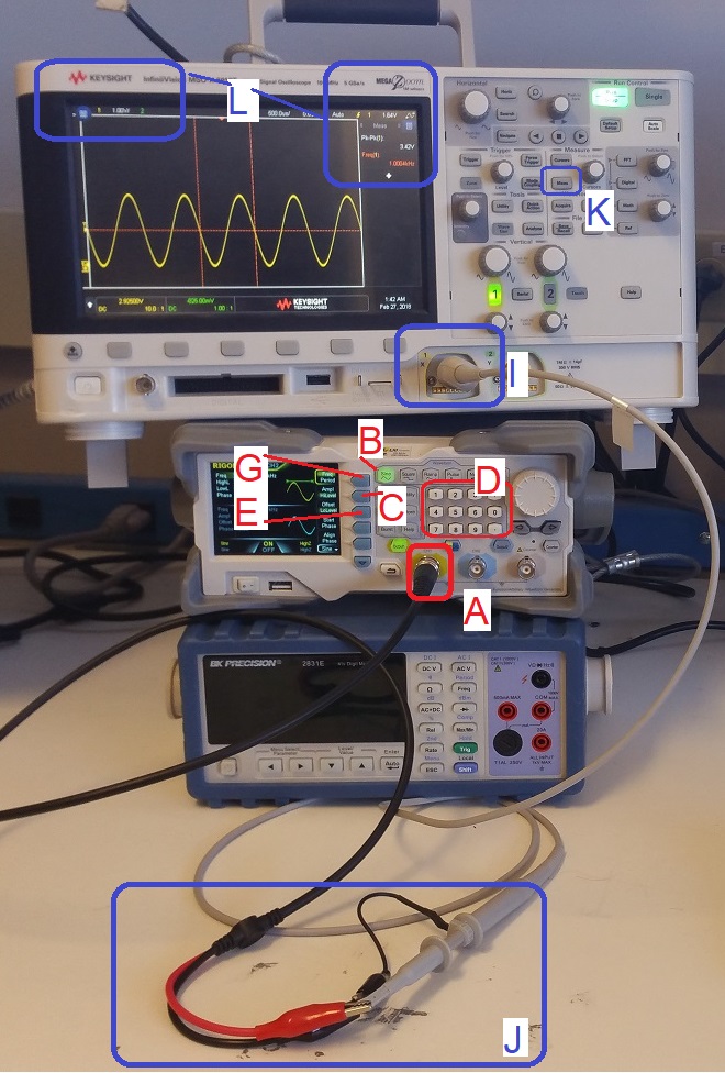
You are now going to use the function generator to send sin waves with varying frequencies into the LPF input and measure the amplitude and phase shift of the output waveform. When you have set up everything correctly it should look like the following picture. The steps in the instructions will walk you though the setup.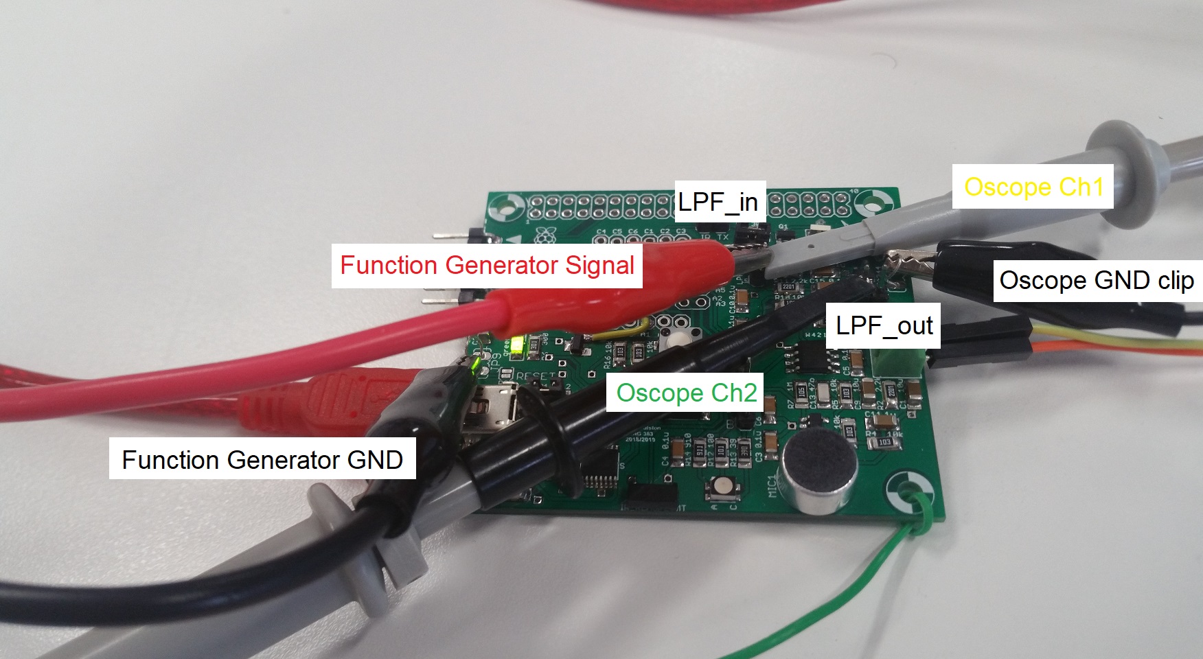
- Install a jumper over the single RC2 pin of the "RC2/LPF_in" header leaving the LPF_in pin available,
- Attach the black ground clip of the function generator to the ground loop of the development board,
- Attach the red signal clip of the function generator to the LPF_in
pin of JP2. It may simplify things to use one of your jumper
wires.
Ch1 probe LPF_in on JP2 header Ch1 ground clip Dev board ground loop Ch1 (scale) 1V Ch2 probe LPF_out on L2A header Ch2 ground clip Disconnect Ch2 (scale) 1V Horizontal (scale) 1 ms Trigger mode Auto Trigger source 1 Trigger slope ↑ Trigger level 1.65V - [Meas] → Type → Phase
- [Meas] → Setting → Source1: 2
- [Meas] → Setting → Source2: 1
- [Meas] → Add Measurement
- [Meas] → Type → Ratio - Full Screen
- [Meas] → Add Measurement
- [↑ Back]
- As the input frequency gets higher (around 2kHz) and the output
waveform decrease in amplitude, measuring the attenuation and phase change
will become almost impossible. When this happens:
- Switch channel 2 into AC coupling, by pressing the channel 2 button and select Coupling: AC. Move the channel 2 ground reference up to the middle of the upper half of the display,
- Use the acquire function to average together several channel 2 waveforms. Acquire → AcqMode → Averaging → #Avgs: 128. You will notice that the waveform updates occur much more slowly and morph whenever you change the frequency. However, you will be able to measure incredibly small amplitudes (down to about -60dB) in this mode,
- [Save/Recall] → Save → Format → 24-bit Bitmap image (*.bmp)
- [Save/Recall] → Save → Press to Save
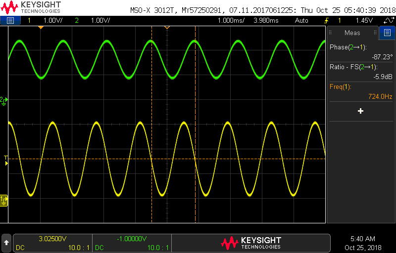
- Include a screen shot with the function generator set to 500Hz. Make sure that the screen shot includes the attenuation and phase measurements.
Note- The Keysight osilloscopes will display the phase in the range [180° to -180°]. So for example, if your LPF generates a -190° phase, the Keysight oscilloscope will display this as 360° - 190° = 170° While is is correct, it will cause your phase graph to have an unsightly discontinuity. Fix this by subtracting 360° from any positive phase reported by the Keysight oscilloscope.
- At low frequencies, the Gain and Phase measurements will not be realiablly reported by the Keysight oscillscope. Please just use the defauly values provided in the Excel file.
- You will see the gain of the Bode plot start to rise at the high frequencies. This is a result of the fact that our circuit has a non-zero amount of inductance For more information check out EEVblog #859 - Bypass Capacitor Tutorial and jump to 11:44.
- Include the Gain and Phase plots as the answer to this question.
Internal Subsystem
We will be focusing on a familiar subsystem today, the pulse width modulation subsystem. Let's get started.Firmware Organization
- In the INTERNAL OSCILLATOR area of the System Module window
- Oscillator Select: Internal oscillator block
- System Clock Select: FOSC
- Internal Clock: 16MHz_HFINTOSC
- Software PLL Enabled: Check
- In the Device Resources area of the project window, expand the Timer option. Double click TMR0,
- In the Device Resources area of the project window, expand the Timer option. Double click TMR2,
- In the Device Resources area of the project window, expand the ECCP option. Double click ECCP1,
- In the Device Resources area of the project window, expand the EUSART option. Double click EUSART1 [PIC10/PIC12/…],
- In the Project Resources area of the project window click on TMR0.
- Enable Timer: ✓
- Enable Prescaler: ✓
- Prescaler: 1:256
- Timer mode: 16-bit
- Clock Source: FOSC/4
- Timer Period: 1ms
- Enable Timer Interrupt: □
- In the Project Resources area of the project window click on EUSART1.
- Enable EUSART: ✓
- Enable Transmit: ✓
- Enable Wake-up: □
- Auto-Baud Detection: □
- Enable Address Detect: □
- Baud Rate: 9600
- Transmission Bits: 8-bit
- Reception Bits: 8-bit
- Clock Polarity: async_noninverted_sync_fallingedge
- Enable Receive: ✓
- Enable EUSART Interrupts: □
- Redirect STDIO to USART ✓
- In the Project Resources area of the project window click on TMR2
- Enable Timer: ✓
- Prescaler: 1:4
- Timer Period: 16us
- In the Project Resources area of the project window click on ECCP1
- ECCP mode: Enhanced PWM
- Timer Select: Timer2
- Duty Cycle: 50%
- Click File → Save All
- Leave the configuration file name as "MyConfig.mc3"
- Click on the "Generate" button in the Project Resources area of the project manager window. Remember that anytime that you make a change to the configuration you must re-generate the supporting files by clicking on the generate button,
- Click on the Project tab in the project manager window, expand the Source Files folder and double click main.c to open it in the editor window,
- Replace the contents of main.c with inlab10.c,
- Compile and download the code to the PIC,
Firmware Experiments
This week's program generates an analog sine wave using the PWM subsystem connected through a low pass filter. Setting the duty cycle of the PWM waveform changes the analog output of the LPF. Doing this fast enough (but not too fast) allows you to produce analog waveforms that you will play back through a speaker. Given the right conditions, when a PWM signal is input into a low pass filter (LPF), the output of the LPF is the average value of the PWM signal. For example, in the image below a 62.5kHz PWM waveform with a 20% duty cycle is applied to a LPF (with corner frequency 724Hz). The LPF will average the PWM waveform generating a DC output with voltage 0.2*3.3V = 0.66V on the output.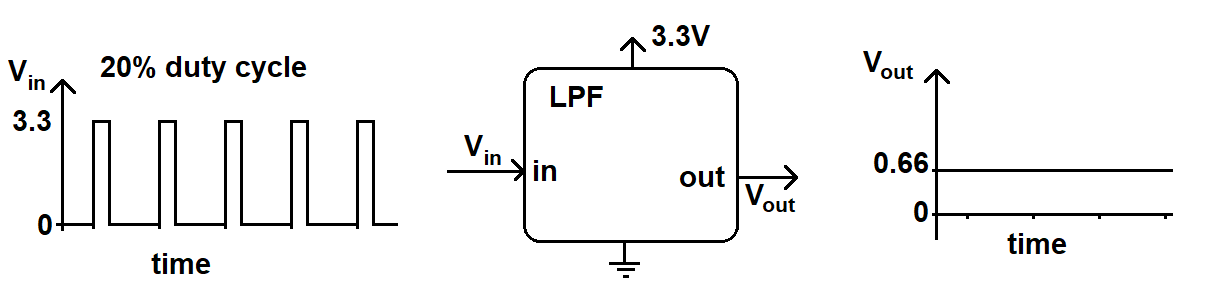
As mentioned, there are right conditions under which a LPF can average a PWM waveform. The most important of these is that the corner frequency of the LPF be much lower than the frequency of the PWM waveform. A general rule of thumb is have the PWM frequency 10 times higher than the corner frequency of LPF. This 1 decade of frequency separation will give a second order filter (like the one on our development board), -40dB of attenuation. This will effectively remove the AC component of the PWM waveform and leave only a residual average. Even with a good LPF you can observe a slight ripple on the output waveform. The amount of ripple is one characteristic of the quality of the DAC conversion.
As a first step to generating a sine wave, we will look at how the the low pass filter averages the duty cycles contained in the sin array. To do this, configure your development board and oscilloscope as follows.- Setup your development board to send the PWM output from RC2 to the LPF_in pin by placing a jumper over the two pin header,
- Use the terminal interface to the development board to generate a sine wave using the "s" option,
Make sure to:Ch1 probe RC2/LPF_in Ch1 ground clip Dev board ground loop Ch1 (scale) 2V Ch2 probe LPF_out on L2A header Ch2 ground clip Dev board ground loop Ch2 (scale) 2V Horizontal (scale) 1ms Trigger mode Auto Trigger source 2 Trigger slope ↑ Trigger level 1.65V - If you enabled AC coupling on Ch2, set it back to DC coupling,
- Align Ch 1 on the second lowest reticule,
- Align Ch 2 on the second lowest reticule on the upper half of the display,
- Align the horizontal position at the second left-most reticule,
- Use the "s" function to change the 8-bit value used to set the
PWM frequency and complete the following table.
Use the Measurement button and find an option to measure the
duty cycle of a waveform.
The LPF output should be a flat line - the oscillations of the PWM
waveform are being averaged out by the LPF. Use the ground
level and the number of volts per division to determine the
LPF output (volt) value.
Duty Cycle (percentage) LoadDutyValue LPF output (volt) 31% 86% 199 22 0.48V 2V
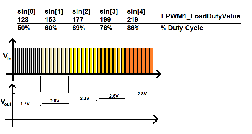
You should notice that Vout does not make an instantaneous transition from one voltage output level to the next. Instead the voltage level gradually changes like a charging RC circuit. We will examine this effect in the next question.-
When the PWM duty cycle changes, the output from the LPF does not
respond instantaneously. The "S" function changes the PWM duty cycle
from 0% to 100% causing the output from the LPF to change from about
0 to 3.3V. Leave the oscilloscope setup the same and perform the
following.
- Use the "S" function to change the PWM duty cycle from 0% to 100%. Note, this creates a step input to the LPF. Measure the rise time, denoted tr of the LPF output. Remember the rise time is the time required for the LPF output to go from 10% of the final value to 90% of the final value. You may find the oscilloscope cursors helpful in making this measurement. You may find it useful to zoom out on the scopes horizontal division (eg 5ms) and to use single mode to capture the rise.
- Screen shot the rise time waveform as your answer to this question.
- Use the equation (familiar to some of you) tr = 2.2 / ω0 where ω0 = 2πf0 to compute the theoretical rise time of the low pass filter.
- Compute the percentage difference between the actual rise time and theoretical rise time as the difference divided by the theoretical times 100. Don't be surprised by signficant different (50% is not unusual).
Spectral content
The following will not be graded as part of the inLab. It is provided in case you would like to experiment with the FFT and gain some additional understanding of the relationship of periodic signals and their spectral content.
In order to convert the PWM waveform into an analog sinusoid, the low pass filter does its best to average the duty cycle of each PWM pulse, however, some small portion of the PWM wave will get through. The "hair spikes" that ride on the sinusoid are the edges of the PWM waveform. The structure of this noise is difficult to understand when viewing the waveform in the time domain. However, by looking at the output sinusoid in the frequency domain using the fast Fourier transform (FFT) of the oscilloscopes, you can understand the spectral composition of the noise and design strategies to reduce it.
For the time being remove channel 2 from the display by pressing the illuminated "2" button twice. Add the FFT to the scope using the following instructions:- [Math] → Function: f(t) → Operator: FFT
- [Math] → Source 1: 1
- [Math] → Span: 100kHz
- [Math] → Center: 50kHz
- [Math] → Display Math → Math1
Experiment with the horizontal adjust for channel 1, adjusting it from 100ms/div to 100us/div. The fidelity of the FFT increases as you provide it with more time-domain data until you saturate the FFT hardware with data, then the FFT just shrinks. Before you move to the next step, make sure that the time scale is 10 ms/div.
- Capture the FFT for the unfiltered PWM waveform (channel 1) and include it as the answer to this question.
- Capture the FFT for the filtered PWM waveform (channel 2) and include it as the answer to this question. To do this you will need to go back into Math mode on the oscilloscope and change the Source setting to channel 2. Note the difference between the two FFTs. Explain why the FFT of the unfiltered PWM waveform (from the previous question) and FFT of the filtered PWM waveform (from this question) look so different. Hint, use the behavior of the Bode plot for the LPF in your explanation.
- Keep the FFT at channel 2 and adjust the span of the FFT to 2k (and center at 1k) and capture the FFT as your answer to this question.
As a first experiment, set the function generator to generate a sine wave at 10kHz. Adjust the FFT to have a span of 100kHz and a center at 40kHz. Adjust the time base to 10ms per division (feel free to adjust the time base to increase/decrease the resolution of the FFT). You may want to turn "off" Ch1 on the oscilloscope so that it does not crowd the screen with the sine wave. Do this by pressing the illuminated "1" button just below the Channel 1 vertical adjust. Note that the ground symbol represent 0dB. Usually only one frequency spike will reach 0dB, this is usually the frequency of the signal that you are applying. The magnitude of the other spikes are measured relative to this level - when in Math mode the scope will display the vertical dB/division scale.
Adjust the frequency of the sine wave on the function generator and observe how the FFT of the sine wave changes. Notice that there is always a large spike on the extreme left side of the screen. For the sine wave input answer the following questions.- How many Hertz are in 1 horizontal division?
- What is the frequency of the large spike on the extreme left of the FFT? What do we call a signal with this frequency?
- Adjust the offset of the sine wave to remove the 1.5V DC offset. Do this by pressing the [Offset/LoLevel] soft key until Offset is selected then enter the offset of 0V using the keypad. What happens to the magnitude of the spike on the extreme left of the FFT?
f(t) = A0/2 + A1*sin(2*πt/T) + A2*sin(2*2*πt/T*t) + A3*sin(3*2*πt/T) + …
The function f(t) is characterized by the coefficients Ai in the Fourier series. Here is the cool part, the FFT function on an oscilloscope shows you these coefficients without having to do any math.
Now switch the function generator to generate a 1kHz square wave. Make sure that the FFT span is 10kHz and the center is 5kHz.- Focus on the large spikes on the FFT. Measure the frequency (in Hz) and amplitude (in dB) of the first three spikes after 1kHz.
- Switch the function generator to generate a ramp. Focus on the large spikes on the FFT. Measure the frequency (in Hz) and amplitude (in dB) of the first three spikes after 1kHz.
- Switch the function generator to generate noise. How many spikes does the FFT look like? Note this is a defining characteristic of noise.