Lab 2 - Signal Display to HDMI
In this lab, you will write a HDMI Video controller in VHDL and implement
it on your FPGA development board. You will be provided a VGA-to-HDMI
module that will automatically format your output for the HDMI output
port on your development board. This HDMI video controller will be tasked
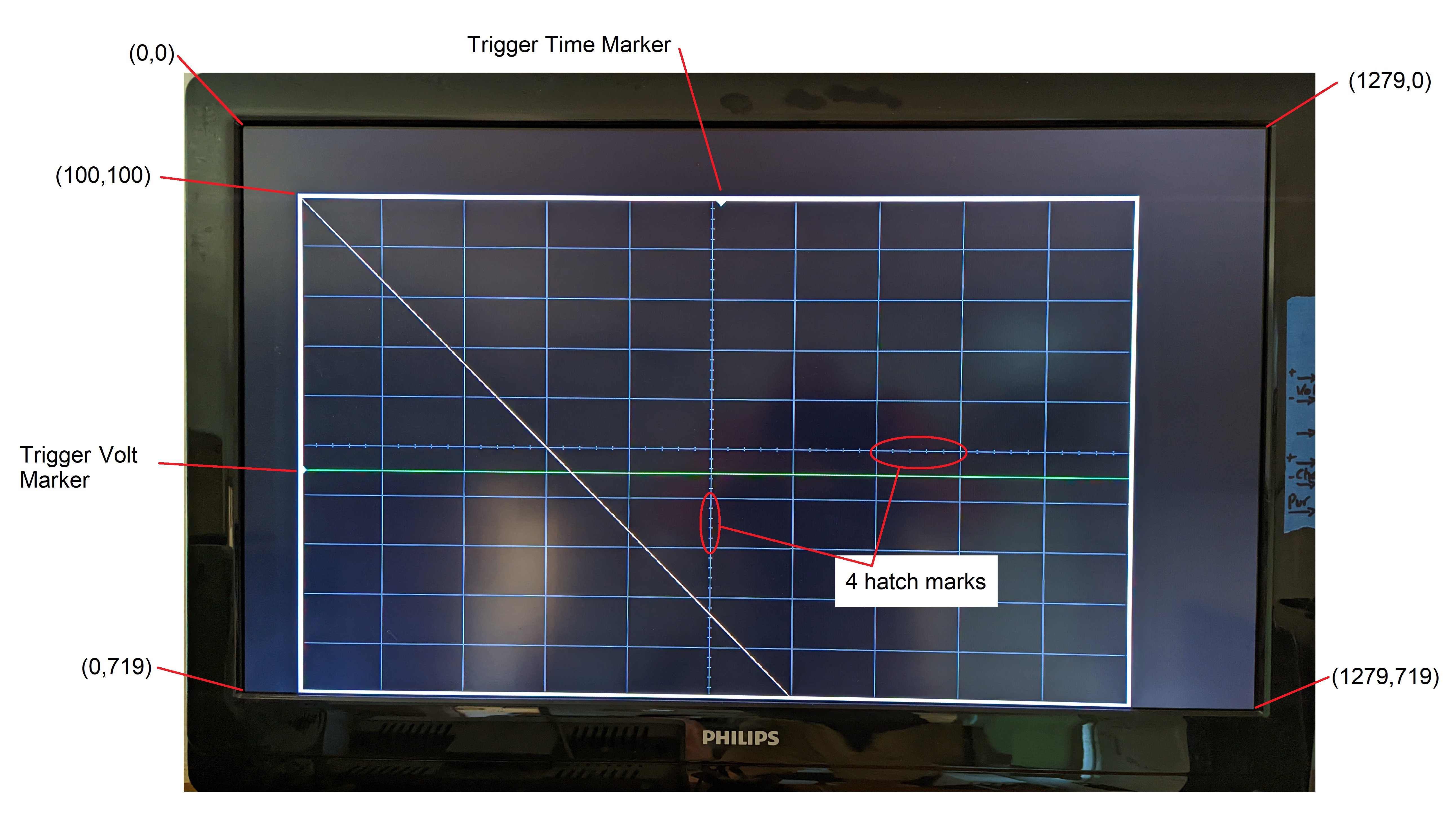
to generate the display portion of an oscilloscope as shown in the
figure below. The scope face consists of a white grid, used to
measure the signals, two trigger markers, and the waveforms. In
this lab the waveforms will be artificially generated by your code,
but in later labs, the waveforms will be generated by incoming
audio waveforms.
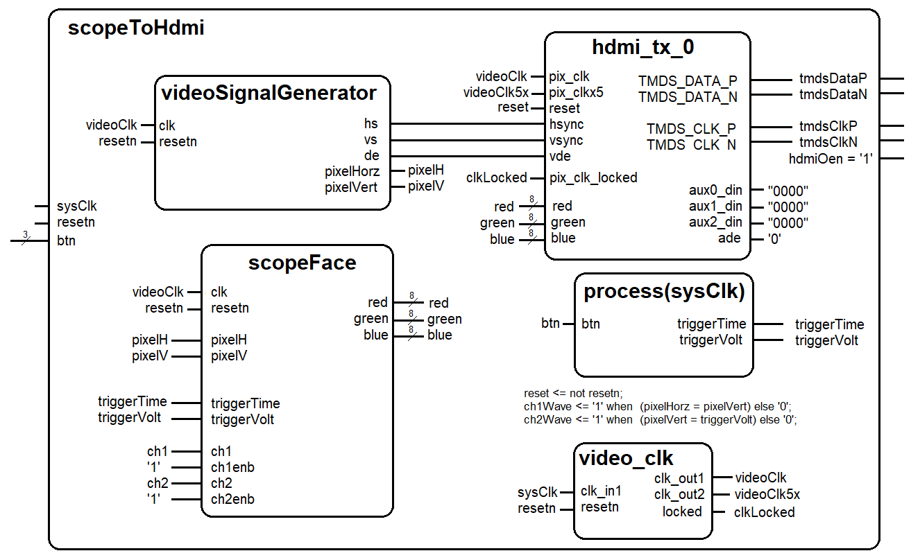
Architecture
The design of the lab is broken down into separate modules, some of which
are provided for you and some which you will need to create. The
interconnection of the modules is illustrated in the following schematic.
When a signal name appears just inside a box, that should should correspond
to the name of that signal in the entity description. Please note
there are a few omissions in the diagram that you should correct
as part of your documentation (see Turn-In section).
VHDL Code
In order to get you going in this lab, some of the VHDL code has been
provided for you. In most cases, you should refrain from changing the
modules given. In order to get a better understanding how these modules
interact with one another, the following section provides a schematic
and the input, output and behavior of some of the modules.
There are two modules which will constitute the majority of your work, videoSignalGenerator
and scopeFace. The following two subsections details the behavior of these
two modules.
The videoSignalGenerator module
The videoSignalGenerator component generates the signals to sweep the
display beam across the display from left to right, and from top to
bottom. The scopeFace component will take the pixelHorz and pixelVert
values and determine what color pixel to place at that location.
entity videoSignalGenerator is
    PORT(
	 clk: in  STD_LOGIC;
         resetn : in  STD_LOGIC;
         hs: out STD_LOGIC;
         vs: out STD_LOGIC;
         de: out STD_LOGIC;
         pixelHorz: out STD_LOGIC_VECTOR(VIDEO_WIDTH_IN_BITS-1 downto 0);
         pixelVert: out STD_LOGIC_VECTOR(VIDEO_WIDTH_IN_BITS-1 downto 0));
end videoSignalGenerator;
| clk | This is the 74.25Mhz videoClk generated by the video_clk component.
|
| resetn | This is the same active low reset signal passed into the top
level Lab1 module.
|
| hs | The h_synch signal for the current row,column position.
|
| vs | The v_synch signal for the current row,column position.
|
| de | The blank signal for the current row,column position. Its
the logical and of the h_blank and v_blank signals.
|
| pixelHorz | The current row on the display that needs a RGB value from this component.
|
| pixelVert | The current column on the display that needs a RGB value from this component.
|
The behavior of the videoSignalGenerator component contains counters which generate:
- h_cnt and v_cnt
- hs and vs
- pixelHorz and pixelVert
- h_activeArea and v_activeArea
The scopeFace module
This component takes in the horizontal and vertical pixel location from the
videoSignalGenerator component and determines the R,G,B value of the pixel
that should be drawn at that location.
entity scopeFace is
    PORT (
  	 clk: in  STD_LOGIC;
         resetn : in  STD_LOGIC;
         pixelHorz : in  STD_LOGIC_VECTOR(VIDEO_WIDTH_IN_BITS-1 downto 0);
         pixelVert : in  STD_LOGIC_VECTOR(VIDEO_WIDTH_IN_BITS-1 downto 0);
         triggerVolt: in STD_LOGIC_VECTOR (VIDEO_WIDTH_IN_BITS-1 downto 0);
         triggerTime: in STD_LOGIC_VECTOR (VIDEO_WIDTH_IN_BITS-1 downto 0);
         red : out  STD_LOGIC_VECTOR(7 downto 0);
         green : out  STD_LOGIC_VECTOR(7 downto 0);
         blue : out  STD_LOGIC_VECTOR(7 downto 0);
         ch1: in STD_LOGIC;
         ch1Enb: in STD_LOGIC;
         ch2: in STD_LOGIC;
         ch2Enb: in STD_LOGIC);
end scopeFace;
| clk | This is the 25Mhz pixel clock generated by the DCM in
the video module.
|
| resetn | This is the same active low reset signal passed into the top level component.
|
| pixelVert | The current row on the display that needs a RGB value from this
component.
|
| pixelHorz | The current column on the display that needs a RGB value from this
component.
|
| triggerVolt | This is a 12-bit value representing the trigger
voltage. This value is passed to the scopeFace module
so that a yellow arrow (see Trigger Level Marker in the
screen show) on the vertical axis.
|
| triggerTime | This is a 12-bit value representing the trigger
time. This value is passed to the scopeFace module
so that a yellow arrow (see Trigger Time Marker in the
screen show) on the horizontal axis.
|
| red | The 8-bit red intensity for this row,column pixel on the screen.
|
| green | The 8-bit green intensity for this row,column pixel on the screen.
|
| blue | The 8-bit blue intensity for this row,column pixel on the screen.
|
| ch1 | This 1-bit signal causes a yellow channel 1 trace to be drawn
on the display at the current pixel location. When this
signal is 0, no channel 1 pixel is drawn.
|
| ch1enb | This 1-bit signal enable the ch1 signal to be drawn.
|
| ch2 | This 1-bit signal causes a green channel 2 trace to be drawn
on the display at the current pixel location. When this
signal is 0, no channel 2 pixel is drawn.
|
| ch2enb | This 1-bit signal enable the ch2 signal to be drawn.
|
The scopeFace component takes in the current row,column coordinates of the
display and generates the R,G,B values at that screen coordinate. For example,
if row,column = 20,20 then the R,G,B output should be 0xFF,0xFF,0xFF (white)
because the upper left corner of the O'scope grid display is white.
The video_clk module
You will need to generate an IP core for this module usin the instructions
in the "howTo 05 Instantiate Clock and HDMI IP" document posted on the
main web page.
The hdmi_tx_0 module
You will need to generate an IP core for this module using the instructions
in the "howTo 05 Instantiate Clock and HDMI IP" document posted on the
main web page.
The scopeToHdmi package
You will need to complete the scopeToHdmi package linked above. Include this
package in this lab's files and in later labs that use these components.
Required Functionality
- You will be asked to show the following simulation results,
- Show a image of your simulation from 0 to 1.2us. This should show the
first line of video with proper hs, h_activeArea, h_cnt and pixelHorz.
- Show a image of your simulation from 0 to 550us. This should show the
first 34 line of video with proper vs, v_activeArea, v_cnt and pixelVert.
- Show a image of your simulation from 0 to 2ms. This should show the
first non-zero RGB values being sent to the display.
- Your code must generate the thick white outline that defines the border
of the oscilloscope. Draw grid in grey (R,G,B) = (0x40, 0x40, 0x40) so that
you have 10 horizontal and 10 vertical divisions. Draw 4 hatch marks in grey
so they evenly split each vertical and horizontal division. Draw the markers
as triangles in cyan (R,G,B) = (0x00, 0xFF, 0xFF).
- The ALINX board has four buttons that you are able to associate with
your design. One of these buttons (PL Key 1) is dedicated to the resetn
function. Use the remaining three keys to manipulate the Trigger Volt Mark
and the Trigger Time Mark as follows:
- Pressing PL_KEY3 decreases the Trigger Volt Mark
- Pressing PL_KEY3 while holding PL_KEY2 increases the Trigger Volt Mark
- Pressing PL_KEY4 increases the Trigger Time Mark
- Pressing PL_KEY4 while holding PL_KEY2 decreases the Trigger Time Mark
- Test the channel functions by:
- Drawing the channel 1 trace (yellow) along a diagonal where (row = column).
- Drawing the channel 2 trace (green) along a horizontal at the same level as
the voltage trigger.
Simulation
You will need to run simulations to make sure that all your
videoSignalGenerator is producing the correct waveforms. I've
included a testbench file and TCL setup script to help you setup
the testbench. The images below are from my simulation output.
You signals may differ slightly in their timing and your
videoSignalGenerator will function just fine. The RGB signal
output really depends on your scopeFace and may differ quite
a bit from what my setup generated.
| Signal | Color | Radix
|
| clk | Green | binary
|
| resetn | Green | binary
|
| h_cnt | Yellow | unsigned
|
| pixelHorz | Yellow | unsigned
|
| h_activeArea | Yellow | binary
|
| hs | Yellow | binary
|
| v_cnt | Yellow | unsigned
|
| pixelVert | Yellow | unsigned
|
| v_activeArea | Yellow | binary
|
| vs | Yellow | binary
|
| de | Green | binary
|
| red | Red | Hexadecimal
|
| green | Green | Hexadecimal
|
| blue | Blue | Hexadecimal
|
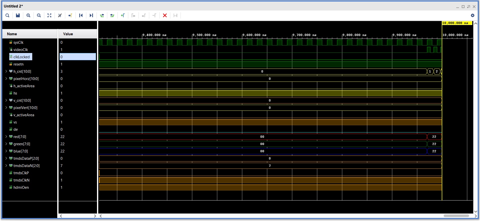
To help you in debugging, I've provided some excerpts from my
testbench simulation. If you right-click on the images and
open in a new window, they will enlarge.
| At 10us |
 |
This shows the clock starting up and the first few hcounts. |
| At 11.5us |
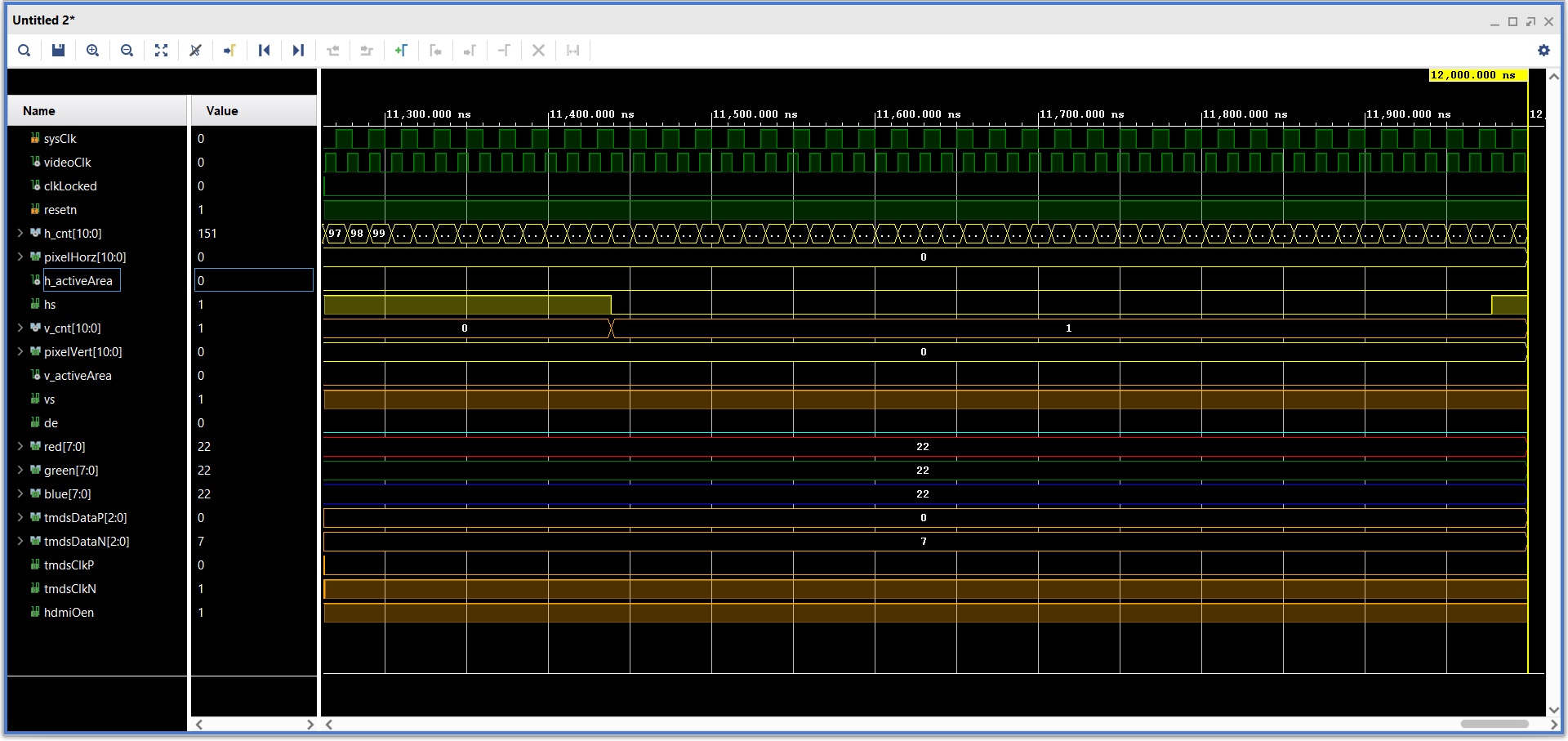 |
This shows the horizontal synch dropping low at h_cnt = 110 and
rising high at ih_cnt = 150. |
| At 32.5us |
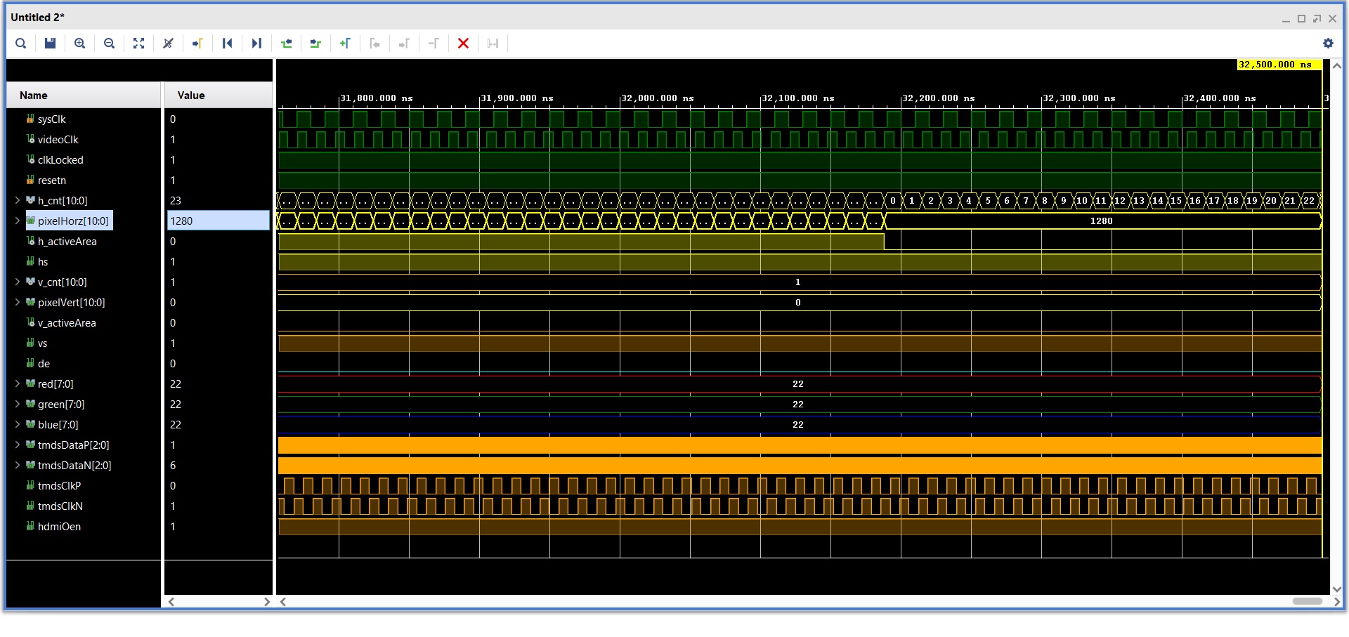 |
This shows h_cnt starting over after counting up to 1649. |
| Up to 700us |
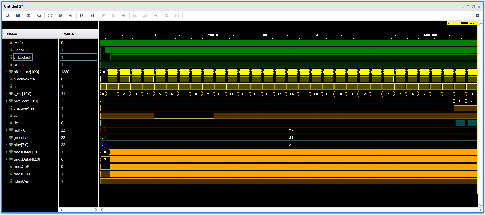 |
This shows the first few rows of video with a proper vsynch and v_active area. |
| At 3ms |
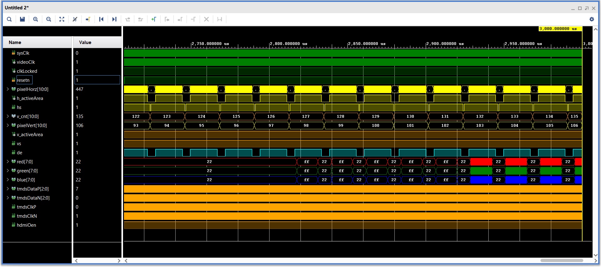 |
This shows the top border of scopeFace being displayed. |
Show a image of your simulation from 0 to 2ms. This should show the
first non-zero RGB values being sent to the display.
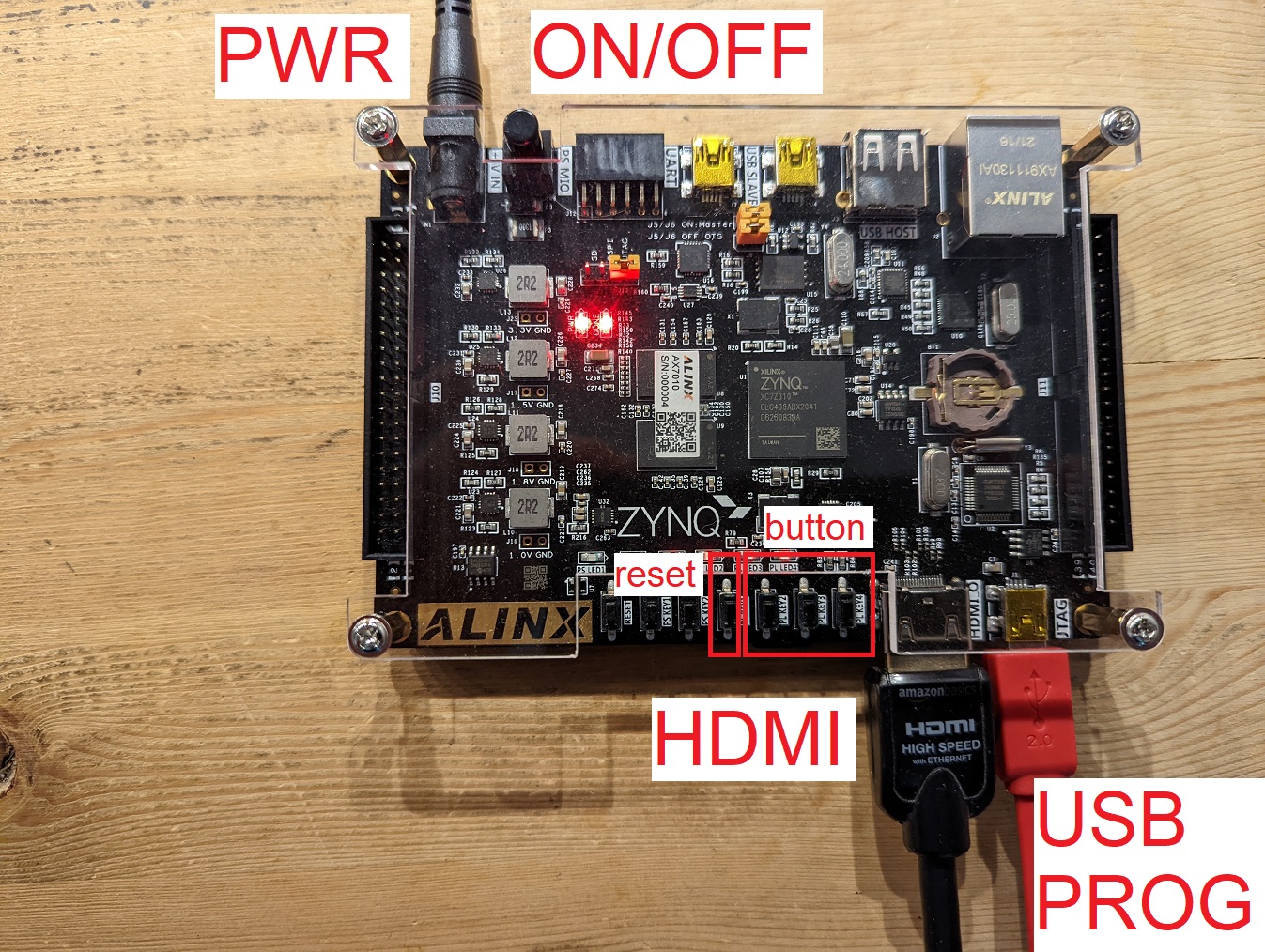
Connecting
Your ALINX board will need to connect to the HDMI port, the JTAG programming
port and the power supply. The image below shows how I made these connections.
The reset and trigger control buttons assigned in the XDC file are also shown.