| Lecture | 21 |
| Class Objectives | An introduction to the AD7606 timing and the datapath and control you will use to extract digitized samples from the AD7606. |
| Handout | AN706 Schematic |
AD7606 Interface
The AD7606 chip that you will interface to the Zynq SoC is housed on the AN706 board manufactured by ALINX. The board, shown below, as a 40 pin header on its lower surface that will mate with the 40 pin headers, J10 or J11 on the ALINX AX7010 board.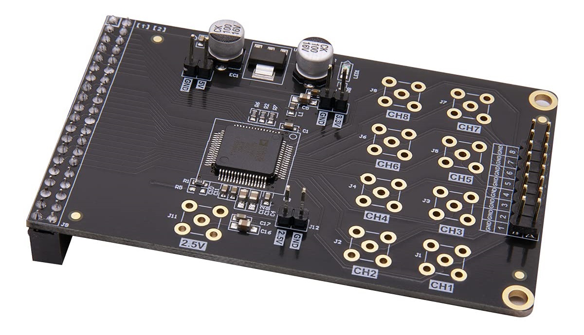
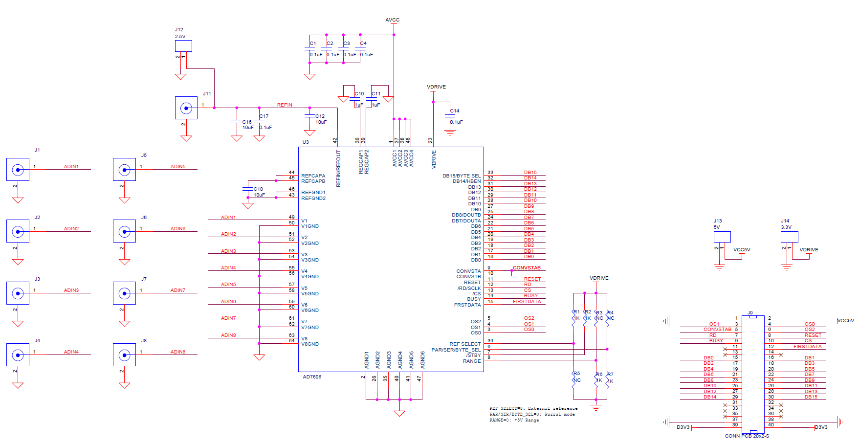
The analog inputs applied to the 8x2 header on the top of the board. The, slightly edited, schematic of the AN706 is shown below.
The 40 pin header, the interface between the AX7010 and AN706 boards is shown at the lower right. Your hardware will be responsible for reading and writing these signals so its essential that you understand how to manipulate them.
Signals
In order to understand the function of the pins, we need to make the following observations from the schematic.- PAR/SER/BYTE SELECT = 0. This means that you will have access to all 16-bits of the converted value at the same time through the DB15:DB0 pins.
- The CONVST A, CONVST B pins are shorted together. This means that all 8 channels are sampled at the same time.
- RANGE = 0. This means that the AD7606 will quantize the inputs over at +5V to -5V range.
- VDRIVE is 3.3V. Note it's the output of the 1117-3.3 chip. A quick search shows that the 1117 is a family low-dropout linear regulator with individual chips offering different, fixed, output voltages. The "-3.3" indicates that the chip on the AN706 board regulates to 3.3V.
| Name | Number of bits | Explaination |
| OS | 3 | Oversampling Mode Pins. Logic inputs. These inputs are used to select the oversampling ratio. OS 2 is the MSB control bit, and OS 0 is the LSB control bit. See the Digital Filter section for more details about the oversampling mode of operation and Table 9 for oversampling bit decoding. |
| Reset | 1 | Reset Input. When set to logic high, the rising edge of RESET resets the AD7606. The device should receive a RESET pulse directly after power-up. The RESET high pulse should typically be 50ns wide. If a RESET pulse is applied during a conversion, the conversion is aborted. If a RESET pulse is applied during a read, the contents of the output registers reset to all zeros. |
| CONVST | 1 | Conversion Start Input A, Conversion Start Input B. Logic inputs. These logic inputs are used to initiate conversions on the analog input channels. For simultaneous sampling of all input channels, CONVST A and CONVST B can be shorted together, and a single convert start signal can be applied. When the CONVST A and CONVST B pin transitions from low to high, the front-end track-and-hold circuitry for the respective analog inputs is set to hold. |
| CS | 1 | Chip Select. This active low logic input frames the data transfer. When both CS and RD are logic low in parallel mode, the DB[15:0] output bus is enabled and the conversion result is output on the parallel data bus lines. |
| RD/SCLK | 1 | Parallel Data Read Control Input When the Parallel Interface Is Selected (RD). When both CS and RD are logic low in parallel mode, the output bus is enabled. |
| BUSY | 1 | Busy Output. This pin transitions to a logic high after both CONVST A and CONVST B rising edges and indicates that the conversion process has started. The BUSY output remains high until the conversion process for all channels is complete. The falling edge of BUSY signals that the conversion data is being latched into the output data registers and is available to read immediatly. Any data read while BUSY is high must be completed before the falling edge of BUSY occurs. Rising edges on CONVST A or CONVST B have no effect while the BUSY signal is high. |
| FIRSTDATA | 1 | We will ignore this output |
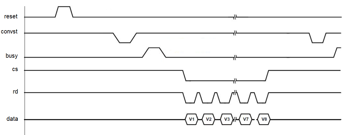
The durations of the pulses is critical to the successful operation of the chip. Looking over the technical documents produces the following values.
| Signal | Time Parameter | Description | Duration | 50Mhz clocks |
| RESET | tRESET | RESET high pulse width | 20ns | |
| CONV | t2 | Minimum CONVST x low pulse | 25ns | |
| BUSY | tCONV | Oversampling off | 4us | |
| RD LOW | t10 | RD low pulse width | 24ns | |
| RD HIGH | t11 | RD high pulse width | 15ns |