| Components
|
Place the following components on the edge of the board:
- Heat sink
- On/Off switch
- Power connector
- Spring terminal block
|
| Have switch near power connector
|
| Have LED near switch
|
| Place heat sink away from controls (fingers that will be
manipulting them)
|
| Put Iset and Vset pots near one another and in a row or column
|
| Place components on 50 mil grid
|
| Align adjacent resistors in rows and column
|
| Each of the four mounting holes should be near one of the board corners
|
| Board
|
| Make the board outline rectangular
|
| Board dimensions should be on 0.1" grid
|
| Make the board outline as small as reasonably possible
|
| Center mounting holes on 0.1" grid
|
| Place mounting holes symmetrically
|
| Route wires on 20 mil grid
|
| Wires
|
| Use 16 mil wires
|
| Do not use the autorouter
|
| Avoid routing wires between close pins
|
| Avoid routing wires between 1206 pads
|
| Avoid 90° bends in wires
|
| Avoid routing on the bottom layer
|
| Use ground via's when convenient
|
| Copper pours
|
| Copper pour ground on the bottom plane
|
| Copper pour power on the top plane
|
| Exactly align top and bottom pour exact
|
| Silk screen
|
| Uniform font and size for part designators (name and value)
|
| Uniform location for part designators on similar parts
|
| Add "on"/"off" text near the switch with correct orientation
|
| Add "CURR" next to Iset pot and "VOLT" next to Vset pot
|
| Add polarity, voltage and current details next to DC power input jack
|
| Optional
|
| Add Blaster ftw
|
This is an individual assignment.
Note: Everyone has access to everyone else's folder - do not make this
the primary repository for your schematic and layout. And do not copy
anyone else's layout - I shouldn't even have to say this.
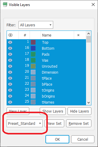
Print your layout as a PDF using the largest scale that allows your
layout to fit on one sheet of 8.5x11 in landscape if you like. Make
sure to have Visible Layers set to Preset_Standard as shown below.
Upload the PDF to Canvas.