EENG 393
In Lab 9 - Board reviewRequirements
Review three designs, assigned to you in class, using the file boardReview.docx. After reviewing a design, upload the completed word document to that person's Google Drive folder.Objective
Critically examine a PCB layout and provide feedback. Utilize feedback on your layout to improve the design.Parts review
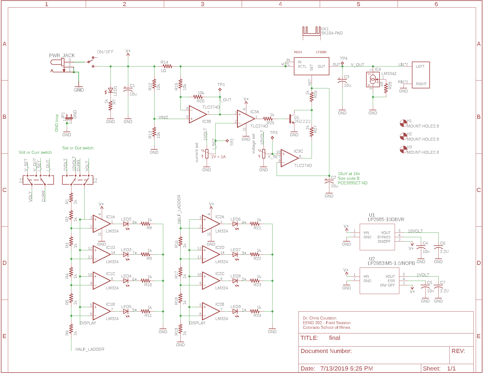
Please generate a bill of materials using the schematic and check it off against the following table. The following table and schematic (scroll down) should resolve any questions that you may have about what footprint to use. You can also look through your bag of parts to see what parts have been provided.| Qty | Value | Device | Package | Parts | Description |
| 9 | LEDCHIPLED_1206 | CHIPLED_1206 | LED1, LED2, LED3, LED4, LED5, LED6, LED7, LED8, LED9 | LED | |
| 2 | SWITCH-DPDT-SMD-AYZ0202 | SWITCH_DPDT_SMD_AYZ0202 | S1, S2 | Double-Pole, Double-Throw (DPDT) Switch | |
| 1 | 100SP1 | 100SP1 | 100SP1 | SW1 | |
| 4 | 10k | R-US_R1206 | R1206 | R12, R13, R15, R20 | RESISTOR, American symbol |
| 2 | 10n | C-USC1206 | C1206 | C4, C5 | CAPACITOR, American symbol |
| 3 | 10u | CPOL-USB | PANASONIC_B | C1, C2, C3 | POLARIZED CAPACITOR, American symbol |
| 22 | 1k | R-US_R1206 | R1206 | R1, R2, R3, R4, R5, R6, R7, R8, R9, R10, R11, R16, R17, R18, R19, R21, R22, R23, R24, R25, R26, R27 | RESISTOR, American symbol |
| 1 | 1Ω | R-US_0411/15 | 0411/15 | R14 | RESISTOR, American symbol |
| 2 | 2.2U | C-USC1206 | C1206 | C6, C7 | CAPACITOR, American symbol |
| 1 | 2N2222 | TRANS_NPN-MMBT2222AL | SOT23-3 | Q1 | NPN transistor |
| 1 | 68 | R-US_R1206 | R1206 | R28 | RESISTOR, American symbol |
| 1 | GND | JP1E | JP1 | JP1 | JUMPER |
| 2 | LM324D | LM324D | SO14 | IC1, IC2 | Quad Op Amp 2.7V to 6.0V Single Supply CMOS |
| 1 | LM334Z | LM334Z | TO92 | IC4 | 3-Terminal Adjustable Current Sources |
| 1 | LP2983IM5-1.0/NOPB | LP2983IM5-1.0/NOPB | MF05A | U2 | |
| 1 | LP2985-10DBVR | LP2985-10DBVR | DBV5 | U1 | |
| 1 | LT3080 | LT3080 | TO-220-5R | REG1 | |
| 1 | MFKDSP | MFKDSP | MFKDSP | JACK1 | |
| 3 | MOUNT-HOLE2.8 | MOUNT-HOLE2.8 | 2,8 | H1, H2, H3 | MOUNTING HOLE with drill center marker |
| 1 | JACK-PLUG0 | SPC4077 | J2 | DC POWER JACK | |
| 2 | EVUF2A | EVUF2A | EVUF | R30,R31 | 9mm Sqaure Rotary Potentiometers |
| 1 | SK104-PAD | SK104-PAD | SK104-PAD | KK1 | HEATSINK manufacturer Fischer/distributor Buerklin |
| 1 | TLC274D | TLC274D | SO14 | IC3 | OP AMP |
| 4 | TPPAD1-13 | TPPAD1-13 | P1-13 | TP1, TP2, TP3, TP4 | Test pad |
Net review
There are a variety of methods that you can employ to help ensure that your layout will be correct. One of these is a net-by-net review of the schematic and layout. The goal is to insure that every signal you placed on the schematic, to connect components, is connecting the corresponding components in the layout.Perform a net-by-net review of your design for next week. This will require a computer running EAGLE CAD, a paper copy of your schematic, a pencil and highlighter. Perform the following steps to get ready for this process.
- Launch EAGLE CAD,
- Open your project,
- Open the schematic and layout side-by-side so that they occupy the entire screen,
- In both the schematic and layout, click Zoom to fit, the magnifying glass with a black rectangle,
- In the schematic, select the information tool,
- Click on a part,
- The Properties pop-up for that part is highlighted in the layout,
- Click Ok to remove the Properties pop-up,
- In the schematic click on the Name tool,
- In the schematic click on a wire,
- The Name pop-up for the wire (showing its name) is highlighted in the layout,
- Click OK to remove the Name pop-up.
To do perform the following set of steps for each net in the schematic.
- Select it using the Name tool,
- Write the net's name on its wire in the schematic,
- If the net has a defined name, then place a check next to the given name,
- For each device that the net (in the schematic) connects to:
- Verify that it is connected in the layout,
- Highlight the schematic pin corresponding to this connection.
- Repeat for all the nets in the schematic.