| Lecture | 15 |
| Class Objectives | Understand the elements and timing of a circuit built using datapath and control. |
Datapath and Control
The datapath and control design methodology break the design of digital systems into two components: a datapath and a control unit. The datapath is responsible for all the data manipulations and the control unit is responsible for sequencing the actions of the datapath. The datapath is constructed from the basic building blocks.A digital system built using the datapath and control design approach is still a digital system whose inputs and outputs can be categorized into Data input, Data output, Control and Status. The digital system shown below consists of two components, a datapath and a control unit.

Datapath Architecture and Timing
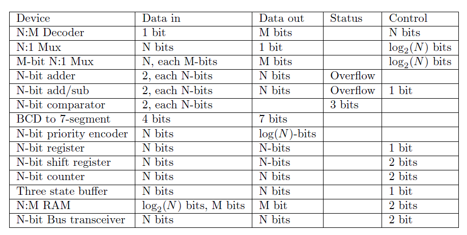
A datapath is constructed from combinational and sequential bulding block. In many cases you can use the basic building blocks provided in the VHDL library used in previous assignments and summarized in the following table.
Each building block that you include in the datapath will have some control bits. You will concationate all of these control bits into a vector and make them an input to the datapath. It will be the control units job to assert the correct control bits at the correct time. To help the control unit accomplish this task, the control unit will need information in the form of status bits from the building blocks inside the datapath. You will concationate all the status bits into a vector and make them an output of the datapath.
Control Unit Architecture and Timing
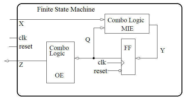
The control unit is a finite state machine (FSM), the most general form of sequential circuit, a circuit whose output is a function of the input and an internal state. In terms of the Figure below, the input is the X vector, the state is the Q vector and the output, the Z vector.
Each of the signals X, Y,Q,Z is a vector, consisting of zero or more bits.
- The X signal is the status word input from the datapath
- The Z signal is the control word output to the datapath
- The Q signal is the state of the control unit. Each bit of Q is the output of a D flip flop. Thus, if Q is six bits wide, then the FSM has six D flip flops.
- The Y signals are called the memory inputs; they are the
data inputs to the D flip flops. The combinational logic circuit generating
the Y signals is called the memory input equations (MIEs). In order to
improve the readability of circuit diagrams, from now on, the clock signal
will not be shown.
In order to define a finite state machine in VHDL, you will need to describe the logic to generate the memory inputs Y and the logic to generate the outputs Z. We will see how to accomplish this soon.FSM Timing
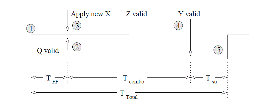
The events occurring in the FSM are referenced to the clock input of the D flip flops inside the FSM. The timing diagram below lists events (numberd in circles) with respect to the clock signal being applied to the Figure above. The following list explains what happens at each of the points in time in the Figure below with respect to the circuit at the top of the page.- Event 1
- Since flip flops sample their inputs on the positive edge of the clock, this point is the beginning of the timing analysis.
- Event 2
- The propagation delay of the flip flops means a small delay occurs between the clock edge and the flip flop outputs, Q, becoming valid. This is the called the propagation delay of the flip flop and denoted T_ff in the diagram below.
- Event 3
- In order to maximize the clocking frequency of the FSM, the new inputs, X, to the FSM should be applied at the same moment that the flip flop outputs become valid.
- Event 4
- According to Figure above, changing Q and X causes the memory inputs to change (the Y signal above). The delay between the application of the new inputs to the MIE logic and Y becoming valid is the propagation delay of the combination logic, denoted Tcombo.
- Event 5 When the Y values are valid, a small delay occurs while the flip flops register their new inputs, denoted Tsu. After this setup time, the FSM is ready for another clock edge.

Datapath and control - timing
There are several important reasons to examine the timing behavior of a datapath and control circuit. First, so that we can make informed predictions about the expected clocking frequency of our circuits. Second, so that we can identify critical paths in our circuit. Third, so that we can develop our intuition about the operation of these complex circuits.
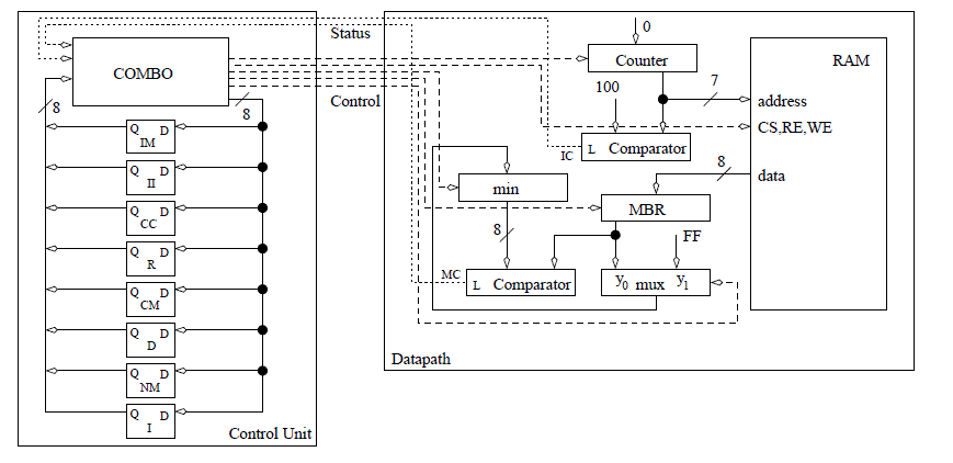
To facilitate a discussion of the timing behavior of the datapath and control circuit, lets examine the circuit from last lecture, the search algorithm for a minimum shown below.
Like we did in our last lecture, we will examine the time its takes, starting from a positive clock edge, to get the next state setup on the flip flops in the FSM. The positive clock edge has two primary effects: It causes the FSM to transition into a new state and it causes the registers in the datapath to latch new values. The propagation delay of the flip flops is referred to as Tp(A). Since the datapath requires a valid control word before it can begin, the critical path includes the output equation logic.
The D flip flops which store the state of the control unit are the input of the OEs. The delay between the application of a valid Q to when the OEs assert their new values is referred to as Tp(B).
The OEs of the FSM are the control word to the datapath telling the elements in the datapath what operation to perform. Sequential logic components do not actually perform their instructed operations until the next clock edge arrives. On the other hand, combinational logic components perform their operations immediately. It is easy to construct datapath instances where the control word effects the status input to the control unit. For example, the control word selects an input of a mux, whose output is routed to a comparator, whose status output is sent to the control unit. Thus, the combinational logic is on the critical path because its delay constrains the maximum clocking frequency. The time difference between the application of a valid control word to the datapath and the status input to the control unit becoming valid is referred to as Tp(C).
The status input to the control unit are routed to the MIE logic. The delay between the status inputs becoming valid and the MIEs becoming valid is referred to as Tp(D).
Once the memory inputs have stabilized, they must be allowed some setup time before the next clock edge. The setup time is referred to as Tp(E).
